Implementation and Dissemination of LED Solid-state Lighting Enabled by Reserach on Advanced Packaging and Assembly Technologies
Summary of Impact
Based on the LED packaging technologies developed at HKUST, the subway company of Hong Kong (MTR) changed the conventional light sources to LEDs, making Hong Kong the first city worldwide with mass adoption of solid-state lighting in the public subway trains and stations. Nowadays more than 95% of lighting systems of MTR use LEDs. With the success of the MTR project, the HKUST LED packaging R&D team was invited by the Foshan Municipal Government in mainland China to establish an engineering center at Foshan. This institution has become one of the most influential engineering centers on solid-state lighting in China.
Underpinning Research
Due to the invention of high-brightness blue LED chips and the development of phosphor-converted white light illumination, LED solid-state lighting (SSL) became possible at the turn of the century. Nevertheless, the applications of LED for general lighting were still limited in the first 5 years of the 21st century due to the lacking of quality packaging solutions, reliable assembly processes, and effective design methodologies. The Center for Advanced Microsystems Packaging (CAMP) and the Electronic Packaging Laboratory (EPACK) are the facilities at HKUST focusing on research advancing technologies for packaging and assemblies of IC devices, optoelectronics, and MEMS/NEMS. CAMP/EPACK initiated their efforts on the R&D of LED packaging and assembly technologies around 15 years ago. The research highlight in this area may be summarized as follows and evidenced by the publications provided in the next section.
Phosphor deposition and silicone encapsulation for LED array packaging - LED light sources usually appear in an array form. The uniformity of packaged chips is essential for ensuring the quality of optical output in terms of brightness and color. The conventional way is to package individual LED chips and then assemble discrete packaged LED components together to form a lighting system. It is rather difficult to achieve uniform brightness and color distribution with the conventional packaging approach. CAMP/EPACK developed batch mode phosphor deposition [R2] and silicone encapsulation [R6] for packaging area array LED chips, which may be implemented at the wafer level or the substrate level. Furthermore, both processes do not require any molding that usually contributes to the majority of the packaging cost. With the two innovative processes that CAMP/EPACK developed, high throughput, high uniformity, and low-cost LED array packaging could be achieved for high quality optical output.
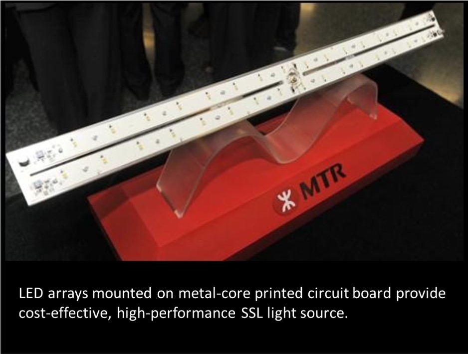
Automated assembly for wide area LED arrays on a flexible printed circuit substrate - Packaged LED components are typically mounted on a metal-core printed circuit board (MCPCB), which is a rigid substrate. Although the surface mount assembly may be an automatic process, due to the size limitation of MCPCB, manually stitching is necessary for wide area LED array assembly. CAMP/EPACK dedicated to develop a surface mount compatible reel-to-reel process that can mount either LED chips or packaged LED components on a continuous flexible printed circuit tape [R4]. This process could be easily implemented for high throughput assemblies of wide area LED arrays in either planar or helical configuration [R3].
Analytical tool for the optimal design of LED arrays - The determination of the spacing between adjacent chips or packaged components of LED arrays is not a straightforward task. The design engineers have to consider the trade-off and optimization among parameters such as power consumption, luminous efficacy, floor illuminance, thermal management, and cost [R1]. In the past, such a design practice was mostly based on experiences or semi-empirical formula. CAMP/EPACK developed an analytical model for the spacing optimization of high-power LED arrays [R5]. This analytical tool can be easily implemented for the optimal design of LED arrays.
Details of the Impact
Based on the R&D outcome of CAMP/EPACK at HKUST, two substantial impacts were resulted in the past decade, one in Hong Kong and the other in mainland China.
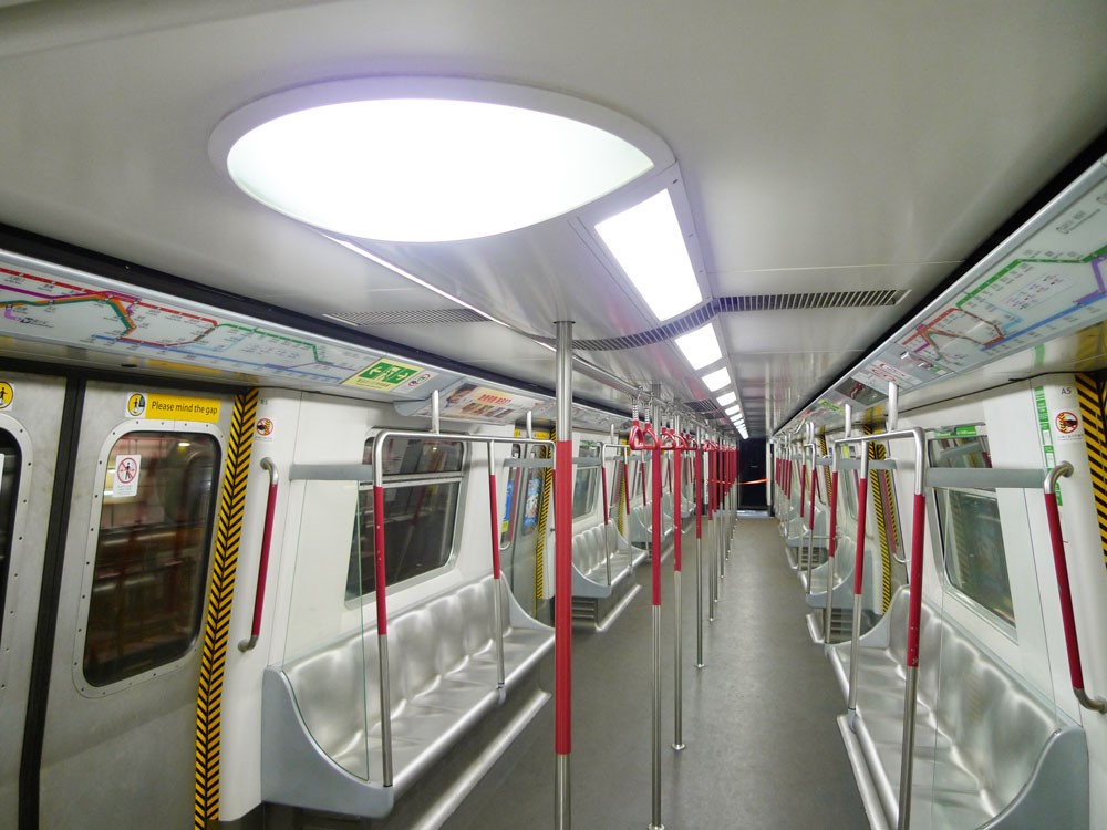
Implementation of solid-state lighting with high brightness LED array modules in the lighting systems of MTR subway - HKUST collaborated with the subway company of Hong Kong, MTR Corp., to implement SSL in the subway systems with the LED packaging and assembly technologies developed at HKUST [R1, R2, R5, R6]. This project was announced to the public in 2006. In the same year the Chinese version of Wikipedia documented this LED SSL trial run of MTR. The underpinning research was actually conducted before then. Due to the company confidentiality and IP issues, HKUST was not allowed to publish papers related to this project until 2006. In the ensuing years the R&D at HKUST continued in parallel for further improvement of LED packaging and assembly. However, their publications in this area always had substantial delay due to the same reason.
After more than two years of continuous test, MTR built up sufficient confidence to upscale the trial run. The Phase 2 trial run was officially announced in a press conference on 12 February, 2009. There was substantial news coverage. In September 2009, MTR hosted the world congress of Community of Metros (CoMet) in Hong Kong and produced a PR video “Green Initiatives – LED Lighting Technology” to publicize their adoption of LED SSL. MTR was considered the first company in the world with practical implementation of LED SSL on subway trains for public mass transportation,
Nowadays more than 95% of subway lighting systems in Hong Kong use LED as light sources. MTR is continuing to install SSL in their lighting systems, and estimates 100% adoption by 2020. At that time the forecasted annual energy reduction due to the implementation of SSL will be at the order of 16,000 MWH. Without the collaboration between HKUST and MTR, such a dramatic energy saving won’t be achieved. The societal impact from the underpinning research of CAMP/EPACK at HKUST is obvious and tangible.
Dissemination of LED SSL through the LED engineering center in mainland China - With the success of the MTR project, HKUST built up the reputation and authority in the communities of LED packaging and SSL technologies [R1-R6]. In 2010, the Nanhai District Government of the Foshan City in mainland China invited HKUST to establish a LED engineering center at Foshan. This is because Foshan has been a national base for the production of conventional light sources such as incandescent light bulbs and fluorescent light tubes. An agreement was signed between HKUST and the Nanhai District Government of the Foshan City in Jun 2010. An initial capital injection of 25M RMB (~3.5M USD) was provided by the Nanhai District Government of the Foshan City and HKUST was committed to build a brand new “HKUST LED-FPD Technology R&D Center” at Foshan. The Center was officially inaugurated for operations in March 2012. The Center consists of 6 laboratories and occupies a space of 1800 sqm. The mission of the Center is to conduct applied research, implement technology transfer, and provide technical services. In 2014, the Center was certified by the China National Accreditation Service (CNAS) for Conformity Assessment, making the Center a top-tier technical service provider in LED. Every year the Center served more than 100 companies on hundreds of projects, all relevant to LED for SSL or flat panel display applications. In addition to paper publications, the Center also filed many technical patents and a number of them have been granted. Over the years, the Center has become one of the most influential engineering centers on LED SSL in China.
Due to the outstanding performance of the Center, the Nanhai District Government decided to further inject resources to elevate the Center to its next stage. A second agreement was signed in 2018, which involved a total funding of 39M RMB (~5.5M USD). In 2019, the Foshan Municipal Government decided to join the Nanhai District Government and sign a third agreement with HKUST. This time the total government funding was increased to 250M RMB (~36M USD). The large scale investment from the government is an endorsement on the performance and the recognition of contributions of the Center to the LED industries. More activities of the Center can be found at its homepage.
References to the Research
[R1] Lee, S. W. R., Lau, C. H., Chan, S. P., Ma, K. Y., Ng, M. H., Ng, Y. W., Lee, K. H., Lo, J. C. C. (2006) “Development and Prototyping of a HB-LED Array Module for Indoor Solid State Lighting,” Proc. 8th IEEE International Conference on High Density Microsystem Design, Packaging & Failure Analysis (HDP), Shanghai, China, 27-30 June, pp. 192-196.
[R2] Lee, K. H., Lee, S. W. R. (2006) “Process Development for Yellow Phosphor Coating on Blue Light Emitting Diodes (LEDs) for White Light Illumination,” Proc. 8th IEEE Electronic Packaging Technology Conference (EPTC), Singapore, 6-8 December, pp. 379-384.
[R3] Lee, S. W. R., Tong, Y. W., Chan, Y. S., Lo, J. C. C., Zhang, R. (2008) “Development of Surface Mount Compatible Reel-to-Reel Assembly Process of LED Arrays for Wide Area General Lighting,” Proc. 3rd IEEE International Microsystems, Packaging, Assembly & Circuits Technology Conference (IMPACT) & 10th International Conference on Electronic Materials & Packaging (EMAP), Taipei, Taiwan, 22-24 October, pp. 255-258.
[R4] Lee, S. W. R., Tong, Y. W., Chan, Y. S., Lo, J. C. C., Zhang, R. (2009) “Process Development and Prototyping for the Assembly of LED Arrays on Flexible Printed Circuit Tape for General Solid State Lighting,” Proc. 59th IEEE Electronic Components & Technology Conference (ECTC), San Diego, CA, 26-29 May, pp. 2137-2142.
[R5] Chan, Y. S., Lee, S. W. R. (2011) “Spacing Optimization of High Power LED Arrays for Solid State Lighting,” Journal of Semiconductors, Vol. 32, No. 1, pp. 014005-1-5.
[R6] Zhang, R., Lee, S. W. R. (2012) “Moldless Encapsulation for LED Wafer Level Packaging using Integrated DRIE Trenches,” Microelectronics Reliability, Vol. 52, pp. 922-932.